The Look Mum No Computer 4051 Plexquencer ( description , purchase ) is an interesting new module. It’s kind of like your basic eight stage Baby-8 style analog sequencer, except that instead of taking a clock signal, it takes three gate inputs (A through C). Those three gates, interpreted as a binary number, tell the module which of the stages to activate. If the inputs count in binary from 0 up to 7 and back to 0, it’ll go through the stages in order (though they’re numbered 1 to 8, which has already caused me some confusion), like a typical sequencer, but if they form a different binary sequence it’ll do different things.

LMNC 4051 Plexquencer
Additionally, there are eight three-position toggle switches. Flip a switch to the left and a gate appears on the Gate Out 1 output when the corresponding stage is active; flip it to the right and the gate appears on Gate Out 2; center it and there’s no gate. Actually what appears on the Gate Out jacks is a logical AND of the stage gates and Input Gate; you can send in, for instance, a rapid gate and get ratcheting effects. One more trick: Normally the CV outputs are in the range 0 to 10 V, but if you put a control voltage into Input Voltage, that will redefine the upper limit, rescaling all the CVs.
There’s a lot of fun stuff you can do with this. Unfortunately there are some design issues, most of which can be corrected easily, but some not so much.
Issues
Reversed gate outputs
There appear to have been a couple of mistakes in laying out the PCB which result in the fact that when you flip a switch to the left, the corresponding gate gets sent to Gate Out 2 instead of Gate Out 1 — though the LED that lights up is the one next to the Gate Out 1 jack.
Input voltage and Input gate normals
Both the Input voltage and Input gate jacks have tip normal connections to +12 V. They are direct connections. As a result, when you insert or remove a plug, it’s likely to momentarily short the +12 V rail to ground. This probably won’t damage anything, but the resultant voltage glitch might briefly upset some modules, and possibly your power supply.
Floating inputs
In testing I noticed some flaky behavior: If I flipped a switch from (say) Gate 1 to Off for some stage while that stage was active, then I expected the corresponding gate should turn off, but instead it would stay on.
Gate thresholds
In CMOS logic, according to the datasheets, the minimum voltage corresponding to a High level (logical True or 1) is 70% of the supply voltage. For +12 V supply, that’s 8.4 V. So that’s the minimum gate amplitude you’re supposed to use to make things work. And that’s a large gate amplitude. Plenty of modules and other equipment will put out gates with only 5 V amplitude.
In fact, the Plexquencer might not even send large enough gates to itself. If the Input Voltage is low enough, then the gates produced by the multiplexer, which go to the AND chip along with the Input Gate, may be below 8.4 V.
So you can expect, if connecting modules that have lower voltage gates or if using the Input Voltage feature, the Plexquencer won’t work properly — you won’t get proper outputs from the multiplexer and/or the AND.
Name is unpronounceable
I mean, it just is.
Remedies
Reversed gate outputs
The easiest fix for the reversed gate outputs is to cut the traces to from the jack board pin header to the Gate Out jacks and add bodge wires to reverse their connections. One trace is on each side of the PCB, so you do have to un-install it. Fifth pin header pad from the bottom should connect to Gate Out 2, fourth from the bottom to Gate Out 1.

Bodge wires for reversed gates
(The adjacent pin header pad looks worse in the photo than in real life, but I did clean it up later. As for the bodge wire on the left, see below.)
Input voltage and Input gate normals
Fixing this would require cutting more traces and adding more bodge wires with resistors — 1k should be fine — in series. I haven’t done that yet, I’ll see how necessary it is.
Floating inputs
I found this behavior would go away if I added 10k pulldown resistors from pins 2 and 5 of the AND chip (or from the cathodes of diodes connected to each of those pins) to ground. That’s not too hard to kludge on the PCB. Or, again, see below.
Gate thresholds
Maybe no fix needed? What I found when I built my Plexquencer was that it worked anyway! Even with input gates as low as 2 V the multiplexer was responding fine, and with Input Voltage as low as 4.5 V the AND was producing correct outputs. Not what the datasheets would lead you to expect, but that’s what I saw.
On the other hand, at least one other builder has reported problems with some gate sources, so it seems likely the behavior with low voltage gates is ill-defined — might work, might not. Maybe it depends on the chip manufacturer, or the batch, or… something.
Inputs In A–C are buffered by TL074 op amps wired as voltage followers. If they were wired instead as comparators with a low threshold, then they’d result in ~10.5 V inputs to the multiplexer whenever an input was above that threshold — always large enough to be treated as High.
That would take care of the inputs to the multiplexer, but there still is the problem of the multiplexer output possibly being too low to activate the AND. For this you could add comparators on each of the three inputs to the CD4081.
Daughterboards
The idea I had was to design a pair of daughterboards. One has a TL074 set up as one voltage follower and three comparators, and it plugs in in place of the TL074 (U1) on the PCB that handles In A–C (and Input voltage).
The second daughterboard replaces the CD4081 (U4). On it is another op amp chip — this time an LM324, because I wanted it powered with a single supply — wired as comparators on each of the three inputs to a CD4081. There also are pulldowns on the inputs from the multiplexer to prevent the flaky behavior mentioned above.
The voltage divider that produces the reference voltage for the comparators is on this board, not on the other, and the other also has no connection to ground. So the two boards have two wires running between them, connecting the reference voltage and ground from the U4 board to the U1 board.
The idea is to solder pairs of 7-position pin sockets in place of the DIP sockets for U1 and U4 on the main PCB, and then plug these two daughterboards into them.
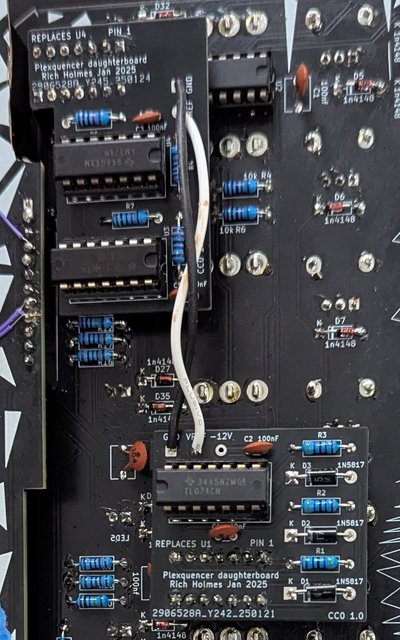
Plexquencer daughterboards
The layout of this is a little dicey. You can’t plug into pin sockets at U4 without encountering interference from the jacks board. So you can see in the above photo how I cut away a bit of the PCB to make room. You have to do that carefully to avoid severing the trace to the first jack. Where by “carefully” I mean “more carefully than I did”. Hence the third bodge wire.
For daughterboard schematics, design files, and Gerbers, see the git repo .
Name is unpronounceable
There is no fix for this.